Research Areas
Our lab explores the cutting edge of photonics and lithography, focusing on four main pillars of research.
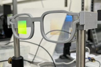
Meta-Optics Element Augmented Reality (AR) Waveguides
Design and fabrication of advanced diffractive optical elements using metasurfaces to enhance the field of view and efficiency of AR display systems.
Explore →
Meta-Optics for AR Waveguides
Overview: This project focuses on overcoming the limitations of traditional refractive optics in Augmented Reality (AR) systems. By leveraging metasurfaces—planar arrays of sub-wavelength nanostructures—we can manipulate the phase, amplitude, and polarization of light with unprecedented control.
Key Research Areas:
- Field of View (FOV) Expansion: Using high-index materials and optimized grating designs to push the FOV limit beyond 50 degrees.
- Efficiency Optimization: Addressing the 'rainbow effect' and uniform light extraction through precise nano-imprint lithography.
- Full-Color Display: Developing multiplexed metasurfaces that can diffract RGB wavelengths simultaneously without crosstalk.
Our approach integrates theoretical simulation (RCWA/FDTD) with extensive cleanroom fabrication (E-beam lithography, RIE) to create lightweight, high-performance AR glasses.
Key Publications
- Reducing eye glow in augmented reality waveguide through topological metagrating designOptical Architectures for Displays and Sensing in Augmented, Virtual, and Mixed Reality, 2025
- 75-4: Late-News Paper: Metalens-Integrated Augmented Reality (AR) Waveguides for Eye-tracking: A Proof of ConceptSID Symposium Digest of Technical Papers, 2024
- Metalens integrated Maxwellian view display for augmented reality glassesOptical Architectures for Displays and Sensing in Augmented, Virtual, and Mixed Reality, 2025
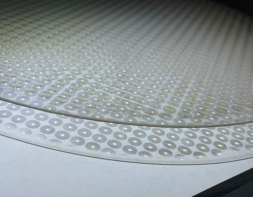
Metalens & Large-Area Meta-Optics
Developing large-area metalens arrays using KrF photolithography with AI-assisted design, achieving high focusing efficiency for imaging, AR displays, and multifocal applications.
Explore →
Metalens & Large-Area Meta-Optics
Overview: Metalenses are planar optical elements composed of sub-wavelength nanostructures that can manipulate light wavefronts with high precision. Our lab pioneers large-area metalens fabrication using deep-UV KrF photolithography, enabling scalable manufacturing beyond traditional e-beam lithography limitations.
Key Research Areas:
- Large-Area Fabrication: Achieving 2cm x 2cm metalens arrays with consistent optical performance using KrF stepper lithography and optimized process parameters.
- AI-Assisted Design: Implementing Intelligent Proximity Correction (IPC) algorithms to compensate for optical proximity effects and achieve precise nanostructure patterning.
- High Focusing Efficiency: Demonstrating 60-64% focusing efficiency for NIR metalenses through Jacobian phase error correction and optimized MTF performance.
- Multifocal Applications: Developing metalens systems for Vergence-Accommodation Conflict (VAC) mitigation in AR/VR displays through precise depth-plane generation.
This research bridges the gap between laboratory-scale metasurface demonstrations and industrial-scale production for consumer optics applications.
Key Publications
- Intelligent Proximity Correction Enabled Large-Area Metasurfaces by KrF PhotolithographyIEEE Access, 2025
- I-line photolithographic metalenses enabled by distributed optical proximity correction with a deep-learning modelOptics Express, 2022
- Metasurfaces on silicon photonic waveguides for simultaneous emission phase and amplitude controlOptics Express, 2023
Resolution Enhancement Technique
Developing computational lithography algorithms, including Source-Mask Optimization (SMO) and OPC, to push the limits of semiconductor manufacturing. Our team has deployed the OPC+ Cloud Service - a general-purpose OPC platform designed for easy access and easy use for everyone.
Explore →Resolution Enhancement Techniques (RET)
Overview: As semiconductor nodes shrink below 3nm, traditional imaging limits pose a massive challenge. Our lab develops advanced computational algorithms to extend the life of current lithography equipment.
Methodologies:
- Source-Mask Optimization (SMO): Simultaneously optimizing the illumination source shape and the mask pattern to maximize the process window.
- Inverse Lithography Technology (ILT): Using pixel-based optimization to create complex, curvilinear mask shapes that print perfectly square wafers features.
- Optical Proximity Correction (OPC): Machine-learning enhanced OPC models to predict and correct layout hotspots faster than conventional rigorous simulation.
This research has direct applications in high-volume manufacturing, aiming to reduce Edge Placement Error (EPE) and improve yield.
OPC+ Cloud Service Implementation

Overview: The OPC+ Cloud Service is a general-purpose OPC platform designed with one goal: making advanced mask correction accessible to everyone. With 'easy access, easy use' as our core philosophy, the platform leverages GPU acceleration and cloud-native architecture to deliver a streamlined freeform mask correction workflow.
Key Features:
- Easy Access: Cloud-based platform accessible from anywhere, eliminating the need for expensive local infrastructure.
- Easy Use: Intuitive 'OPC for Everyone' interface - no scripting or deep technical knowledge required. Simply upload your layout and configure parameters.
- General-Purpose Freeform OPC: Native support for curvilinear masks, essential for photonic integrated circuits and advanced semiconductor designs.
- GPU-Accelerated Performance: CUDA Multi-Stream technology delivers significant speedup compared to traditional CPU-based methods.
- Cloud-Native Architecture: Kubernetes-based elastic scaling ensures optimal resource utilization and predictable performance.
- Industry Standards: Seamless integration with existing workflows through GDS/OASIS format support.
Platform Goals:
- Democratize access to advanced OPC technology
- Remove complexity barriers in mask correction
- Support both semiconductor and photonic manufacturing
Access the Platform:
View on GitHub View BrochureContact us for platform access and collaboration opportunities.
Key Publications
- High contrast EUV imaging enabled by topological quasi phase-only masksOptics Express, 2026
- A Novel Optical Proximity Correction Machine Learning Model Using a Single-Flow Convolutional Feedback Networks with Customized AttentionIEEE Access, 2024
- Reducing M3D effects in EUV masks by balancing diffraction ordersOptical and EUV Nanolithography XXXVIII, 2025
Quantum Annealing
Applying quantum computing paradigms to solve complex optimization problems in inverse lithography and mask synthesis, achieving faster convergence and better pattern fidelity.
Explore →Quantum Annealing for Lithography
Overview: Optimization problems in lithography (like SMO and ILT) are NP-hard and computationally expensive. We explore Quantum Annealing (QA) as a specialized solver to find global minima more efficiently than classical simulated annealing.
Research Highlights:
- Ising Model Formulation: Mapping the lithography mask optimization problem onto the Ising model suitable for D-Wave quantum annealers.
- Hybrid Algorithms: Combining classical gradient descent with quantum sampling to overcome the qubit connectivity limitations of current hardware.
- Benchmarking: Demonstrating significant speedup in convergence time for complex 2D mask patterns compared to traditional CPU/GPU clusters.
Key Publications
- Inverse reticle optimization with quantum annealing and hybrid solversIEEE Access, 2024
- Tackling data inconsistency and runtime issues in inverse lithography technology (ILT) with comparative convergence studyDTCO and Computational Patterning III, 2024
- Practical inverse mask synthesis via data-efficient physics-informed neural networks (PINN) modelDTCO and Computational Patterning IV, 2025